
Author Affiliations
Abstract
1 School of Physics, Peking University, Beijing 100871, China
2 The State Key Laboratory for Artificial Microstructures and Mesoscopic Physics, School of Physics & Center for Quantitative Biology, Academy for Advanced Interdisciplinary Studies, Peking University, Beijing 100871, China
3 Academy for Advanced Interdisciplinary Studies, Peking University, Beijing 100871, China
4 Wenzhou Institute, University of Chinese Academy of Sciences, Wenzhou 325001, China
Chirality plays an important role in biological processes, and enantiomers often possess similar physical properties and different physiologic functions. In recent years, chiral detection of enantiomers become a popular topic. Plasmonic metasurfaces enhance weak inherent chiral effects of biomolecules, so they are used in chiral detection. Artificial intelligence algorithm makes a lot of contribution to many aspects of nanophotonics. Here, we propose a nanostructure design method based on reinforcement learning and devise chiral nanostructures to distinguish enantiomers. The algorithm finds out the metallic nanostructures with a sharp peak in circular dichroism spectra and emphasizes the frequency shifts caused by nearfield interaction of nanostructures and biomolecules. Our work inspires universal and efficient machine-learning methods for nanophotonic design.
chiral detection metasurface deep learning cathodoluminescence Opto-Electronic Science
2023, 2(1): 220019

Author Affiliations
Abstract
School of Physics, State Key Lab for Mesoscopic Physics, Academy for Advanced Interdisciplinary Studies, Collaborative Innovation Center of Quantum Matter, Yangtze Delta Institute of Optoelectronics, and Nano-optoelectronics Frontier Center of Ministry of Education, Peking University, Beijing 100871, China
The manipulation of polarization states beyond the optical limit presents advantages in various applications. Considerable progress has been made in the design of meta-waveplates for on-demand polarization transformation, realized by numerical simulations and parameter sweep methodologies. However, due to the limited freedom in these classical strategies, particular challenges arise from the emerging requirement for multiplex optical devices and multidimensional manipulation of light, which urge for a large number of different nanostructures with great polarization control capability. Here, we demonstrate a set of self-designed arbitrary wave plates with a high polarization conversion efficiency. We combine Bayesian optimization and deep neural networks to design perfect half- and quarter-waveplates based on metallic nanostructures, which experimentally demonstrate excellent polarization control functionalities with the conversion ratios of 85% and 90%. More broadly, we develop a comprehensive wave plate database consisting of various metallic nanostructures with high polarization conversion efficiency, accompanying a flexible tuning of phase shifts () and group delays (0–10 fs), and construct an achromatic metalens based on this database. Owing to the versatility and excellent performance, our self-designed wave plates can promote the performance of multiplexed broadband metasurfaces and find potential applications in compact optical devices and polarization division multiplexing optical communications.
Photonics Research
2023, 11(5): 695
Author Affiliations
Abstract
1 School of Physics, State Key Lab for Mesoscopic Physics, Academy for Advanced Interdisciplinary Studies, Collaborative Innovation Center of Quantum Matter, and Nano-optoelectronics Frontier Center of Ministry of Education, Peking University Yangtze Delta Institute of Optoelectronics, Peking University, Beijing 100871, China
2 National Laboratory of Solid State Microstructures, Department of Materials Science and Engineering, Nanjing University, Nanjing 210093, China
3 College of Chemistry and Molecular Engineering, Peking University, Beijing 100871, China
4 Department of Physics and HKU-UCAS Joint Institute for Theoretical and Computational Physics at Hong Kong, the University of Hong Kong, Pokfulam Road, Hong Kong, China
![]()
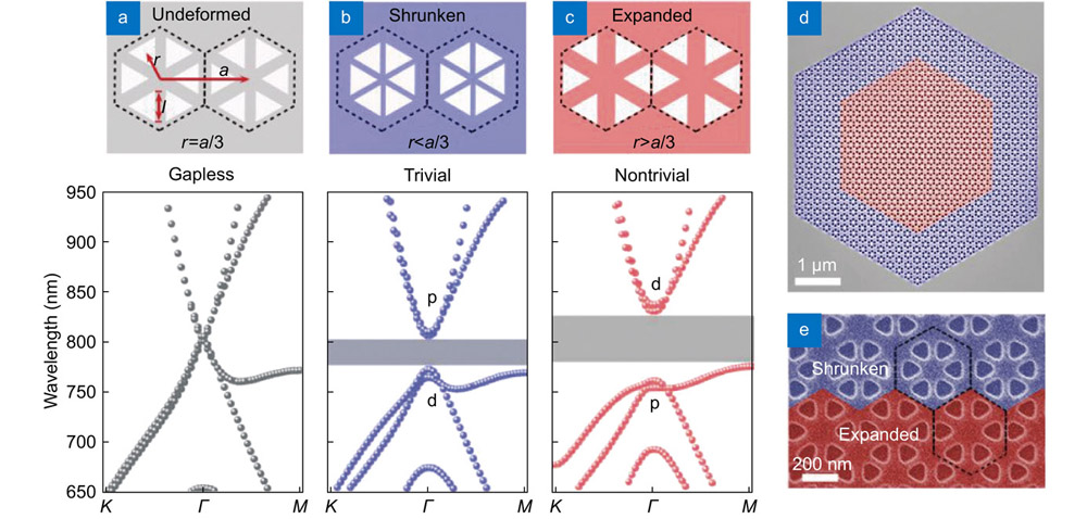
![]() Photonic topological insulators with robust boundary states can enable great applications for optical communication and quantum emission, such as unidirectional waveguide and single-mode laser. However, because of the diffraction limit of light, the physical insight of topological resonance remains unexplored in detail, like the dark line that exists with the crystalline symmetry-protected topological edge state. Here, we experimentally observe the dark line of the Z2 photonic topological insulator in the visible range by photoluminescence and specify its location by cathodoluminescence characterization, and elucidate its mechanism with the p-d orbital electromagnetic field distribution which calculated by numerical simulation. Our investigation provides a deeper understanding of Z2 topological edge states and may have great significance to the design of future on-chip topological devices.
Photonic topological insulators with robust boundary states can enable great applications for optical communication and quantum emission, such as unidirectional waveguide and single-mode laser. However, because of the diffraction limit of light, the physical insight of topological resonance remains unexplored in detail, like the dark line that exists with the crystalline symmetry-protected topological edge state. Here, we experimentally observe the dark line of the Z2 photonic topological insulator in the visible range by photoluminescence and specify its location by cathodoluminescence characterization, and elucidate its mechanism with the p-d orbital electromagnetic field distribution which calculated by numerical simulation. Our investigation provides a deeper understanding of Z2 topological edge states and may have great significance to the design of future on-chip topological devices.
photonic topological insulator edge state cathodoluminescence TMDC Opto-Electronic Advances
2022, 5(4): 210015

Author Affiliations
Abstract
School of Physics, State Key Laboratory for Mesoscopic Physics, Academy for Advanced Interdisciplinary Studies, Collaborative Innovation Center of Quantum Matter, and Nano-optoelectronics Frontier Center of Ministry of Education, Peking University, Beijing 100871, China
Quantum information technology requires bright and stable single-photon emitters (SPEs). As a promising single-photon source, SPEs in layered hexagonal boron nitride (hBN) have attracted much attention recently for their high brightness and excellent optical stability at room temperature. In this review, the physical mechanisms and the recent progress of the quantum emission of hBN are reviewed, and the various techniques to fabricate high-quality SPEs in hBN are summarized. The latest development and applications based on SPEs in hBN in emerging areas are discussed. This review focuses on the modulation of SPEs in hBN and discusses possible research directions for future device applications.
quantum emission single-photon emitter hexagonal boron nitride two-dimensional materials quantum nanophotonics Chinese Optics Letters
2022, 20(3): 032701
将光子计数技术与单像素成像结合的单光子压缩成像方法具有成本低、灵敏度高的特点,但该方法使用传统压缩重建算法时重建时间长。基于深度学习的压缩重建网络不仅实现了快速重建,而且可获得更好的重建质量。最近用于单像素成像的压缩重建网络主要基于光探测器工作在模拟方式,采用无噪声或带有加性高斯白噪声的系统仿真数据进行训练。对此,建立了单光子压缩成像系统噪声模型,提出了一种用于单光子压缩成像的抗噪声重建网络(RN)训练方法,使用含有泊松噪声的测量值仿真数据对神经网络进行训练,并搭建单光子压缩成像系统进行验证。实验结果表明,RN能明显提高各种已有压缩重建网络的图像重建质量。在此基础上,提出了一种用于单光子压缩成像的抗噪重建网络(RPN-net),该网络采用跨越式连接结构与阶段式训练方法,实验结果表明其重建性能优于现有的压缩重建网络。
成像系统 压缩感知 光子计数技术 单光子压缩成像 深度学习 泊松噪声 激光与光电子学进展
2022, 59(4): 0411003

Author Affiliations
Abstract
1 School of Physics, State Key Laboratory for Mesoscopic Physics, Academy for Advanced Interdisciplinary Studies, and Nano-optoelectronics Frontier Center of Ministry of Education, Peking University, Beijing 100871, China
2 Key Laboratory of Photochemical Conversion and Optoelectronic Materials, Technical Institute of Physics and Chemistry, Chinese Academy of Sciences, Beijing 100190, China
3 State Key Laboratory of Precision Measurement Technology and Instruments, Department of Precision Instruments, Tsinghua University, Beijing 100084, China
4 Collaborative Innovation Center of Quantum Matter, Beijing, China
With the recent development of the metasurface, generating an optical vortex in optical far or near fields is realized in various ways. However, to generate vortices in both the near and far fields simultaneously is still a challenge, which has great potential in the future compact and versatile photonic system. Here, a bi-channel optical vortex generator in both the near and far fields is proposed and demonstrated within a single metasurface, where the surface plasmon vortex and the far-field optical vortex can be simultaneously generated under circularly polarized light. The ability of generating vortices with arbitrary topological charges is experimentally demonstrated, which agrees well with simulations. This approach provides great freedom to integrate different vortex generators in a single device, and offers new opportunities for integrated optical communications, trapping, and other related fields.
Photonics Research
2020, 8(6): 06000986
在进行高分辨率成像时,由于需要大量的测量和图像重建计算,单光子压缩成像需要较长的时间。提出了一种采样和重建集成的残差编解码网络SRIED-Net用于单光子压缩成像。将二值化的全连接层作为网络的第一层,并将其训练成二进制的测量矩阵,直接加载到数字微镜阵列上以实现高效压缩采样。除第一层外的其余网络都用于快速重建压缩感知图像。通过一系列的仿真和系统实验比较了压缩采样率、测量矩阵和重建算法对成像性能的影响。实验结果表明,SRIED-Net在低测量率下优于目前比较先进的迭代算法TVAL3,在高测量率下与TVAL3的效果很接近,在所有测量率下都优于目前常见的几种基于深度学习的方法。
成像系统 单光子成像 单光子压缩成像 压缩感知 深度学习
Author Affiliations
Abstract
1 School of Physics, State Key Laboratory for Mesoscopic Physics, Academy for Advanced Interdisciplinary Studies, and Nano-optoelectronics Frontier Center of Ministry of Education, Peking University, Beijing 100871, China
2 Department of Materials Science and Engineering, College of Engineering, Peking University, Beijing 100871, China
3 Department of Materials Science and NanoEngineering, Rice University, 6100 Main Street, Houston, TX 77005, USA
4 Collaborative Innovation Center of Quantum Matter, Beijing 100871, China
Manipulation of light-matter interaction is critical in modern physics, especially in the strong coupling regime, where the generated half-light, half-matter bosonic quasiparticles as polaritons are important for fundamental quantum science and applications of optoelectronics and nonlinear optics. Two-dimensional transition metal dichalcogenides (TMDs) are ideal platforms to investigate the strong coupling because of their huge exciton binding energy and large absorption coefficients. Further studies on strong exciton-plasmon coupling by combining TMDs with metallic nanostructures have generated broad interests in recent years. However, because of the huge plasmon radiative damping, the observation of strong coupling is significantly limited at room temperature. Here, we demonstrate that a large Rabi splitting (~300 meV) can be achieved at ambient conditions in the strong coupling regime by embedding Ag-WS2 heterostructure in an optical microcavity. The generated quasiparticle with part-plasmon, part-exciton and part-light is analyzed with Hopfield coefficients that are calculated by using three-coupled oscillator model. The resulted plasmon-exciton polaritonic hybrid states can efficiently enlarge the obtained Rabi splitting, which paves the way for the practical applications of polaritonic devices based on ultrathin materials.
Rabi splitting strong coupling transition metal dichalcogenides optical microcavity surface plasmons Opto-Electronic Advances
2019, 2(5): 190008
Author Affiliations
Abstract
School of Physics, State Key Lab for Mesoscopic Physics, Academy for Advanced Interdisciplinary Studies, Collaborative Innovation Center of Quantum Matter, Peking University, Beijing 100871, China
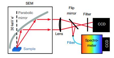
Cathodoluminescence (CL) as a radiative light produced by an electron beam exciting a luminescent material, has been widely used in imaging and spectroscopic detection of semiconductor, mineral and biological samples with an ultrahigh spatial resolution. Conventional CL spectroscopy shows an excellent performance in characterization of traditional material luminescence, such as spatial composition variations and fluorescent displays. With the development of nanotechnology, advances of modern microscopy enable CL technique to obtain deep valuable insight of the testing sample, and further extend its applications in the material science, especially for opto-electronic investigations at nanoscale. In this article, we review the study of CL microscopy applied in semiconductor nanostructures for the dislocation, carrier diffusion, band structure, doping level and exciton recombination. Then advantages of CL in revealing and manipulating surface plasmon resonances of metallic nanoantennas are discussed. Finally, the challenge of CL technology is summarized, and potential CL applications for the future opto-electronic study are proposed.
cathodoluminescence microscopy semiconductor metallic nanostructures surface plasmons Opto-Electronic Advances
2018, 1(4): 180007
北京大学物理学院人工微结构和介观物理国家重点实验室, 北京 100871
表面等离激元因具有能突破光学衍射极限、表面局域性和近场增强等奇特的光学性质,被广泛应用于光伏、光催化和光电探测等研究领域。将具有高效光捕获特性的表面等离激元与传统半导体器件相结合,可以极大地提高传统半导体器件的效率,具有重要的应用价值。由局域表面等离激元弛豫产生的热电子是将太阳能转化为电能或化学能的关键,因此从微观上研究表面等离激元热电子的产生及弛豫过程对于设计高效率表面等离激元纳米光电器件具有重要意义。综述了表面等离激元热电子的激发及其在金属-半导体材料界面处的超快动力学过程的研究进展,分析了目前存在的主要问题并对其未来的发展前景进行了展望。
表面光学 表面等离激元 热电子 异质结 抽运-探测技术 激光与光电子学进展
2017, 54(3): 030002


